
Description
Product Overview
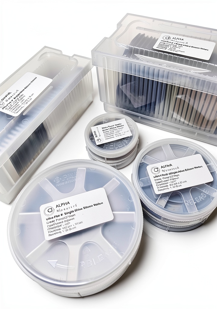
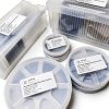
The Alpha Nanotech Prime‑Grade 4” Silicon Wafer is engineered for high‑precision laboratory and research environments where material consistency and surface quality are paramount. Manufactured by Alpha Nanotech Inc., a trusted name in semiconductor substrates, this wafer features a P‑type doping profile achieved through boron implantation, delivering reliable electrical characteristics for a wide range of applications. The wafer measures 4 inches in diameter with a thickness of 525 µm, providing a robust platform for both experimental and production‑scale processes.
Key physical specifications include a polished front surface that ensures low optical scatter and an etched back surface that facilitates easy handling and mounting. Surface flatness parameters are tightly controlled: Total Integrated Roughness (TIR) is less than 3 µm, Total Thickness Variation (TTV) is under 10 µm, Bow (BOW) remains below 10 µm, and surface roughness is kept under 0.5 nm. These tolerances guarantee that the wafer will perform consistently across multiple cycles of photolithography, ion implantation, and other semiconductor fabrication steps.
![[Product front view showing all components]](https://www.civro.store/wp-content/uploads/2026/07/81288f9a1aef453492af927843aba616.jpg)
Usage
Designed for autoradiography supplies, this wafer excels in applications that require high‑resolution imaging of radioactive samples. Researchers in molecular biology, radiochemistry, and materials science can leverage the wafer’s pristine surface to achieve clear, reproducible autoradiographic prints. Beyond autoradiography, the wafer is suitable for semiconductor device prototyping, thin‑film deposition, and surface analysis techniques such as atomic force microscopy (AFM) and scanning electron microscopy (SEM).
Its prime‑grade classification makes it an ideal choice for academic laboratories, industrial R&D facilities, and specialized testing centers that demand strict adherence to material standards. The wafer’s dimensions and doping type are compatible with standard wafer handling equipment, including robotic loaders, spin coaters, and vacuum chucks, ensuring seamless integration into existing workflows.
Why Choose Us
Alpha Nanotech’s commitment to quality is reflected in every wafer we produce. Each batch undergoes rigorous inspection using high‑resolution interferometry and surface profilometry to verify that TIR, TTV, BOW, and roughness specifications are met or exceeded. Our manufacturing process incorporates clean‑room protocols that minimize particulate contamination, preserving the wafer’s surface integrity from the moment it leaves the fab to the point of delivery.
We understand that scientific research often operates on tight timelines. To support our customers, we provide fast order processing, reliable shipping, and responsive technical support staffed by engineers familiar with semiconductor materials. Should you encounter any issues, our after‑sales service team is ready to assist with troubleshooting, replacement, or guidance on optimal usage practices.
Key Features
- Prime‑grade P‑type silicon ensures consistent electrical performance for sensitive experiments.
- Polished front surface reduces optical scattering, enhancing image clarity in autoradiography.
- Etched back surface provides easy handling and secure mounting on standard wafer carriers.
- Strict flatness tolerances (TIR < 3 µm, TTV < 10 µm, BOW < 10 µm) guarantee repeatable results across multiple processes.
- Dedicated technical support and rapid replacement service give you confidence in long‑term projects.
FAQ
What does “Prime‑Grade” mean for this wafer?
Prime‑Grade indicates that the wafer meets the highest industry standards for purity, crystallographic orientation, and surface flatness. It is suitable for applications where any deviation in material quality could affect experimental outcomes.
Can this wafer be used for both autoradiography and semiconductor fabrication?
Yes. The wafer’s P‑type doping, precise thickness, and low surface roughness make it versatile for imaging techniques as well as for device prototyping, thin‑film deposition, and other semiconductor processes.
What handling precautions should be taken to avoid damaging the wafer?
Handle the wafer with clean, lint‑free gloves and use standard wafer carriers or vacuum chucks designed for 4‑inch substrates. Avoid contact with abrasive materials and store the wafer in a static‑controlled environment to prevent contamination.
Is the wafer compatible with standard photolithography equipment?
Absolutely. Its 4‑inch diameter and 525 µm thickness conform to the specifications of most photolithography tools, spin coaters, and exposure systems used in research and small‑scale production.
What is the warranty or return policy for this product?
Alpha Nanotech offers a 30‑day warranty against manufacturing defects. If the wafer arrives damaged or does not meet the stated specifications, contact our support team for a replacement or refund.
By choosing the Alpha Nanotech Prime‑Grade 4” Silicon Wafer, you invest in a substrate that delivers reliability, precision, and support throughout the lifecycle of your research or development project. Whether you are imaging radioactive samples, fabricating prototype devices, or conducting surface analysis, this wafer provides the foundation you need for success.

 Pop Culture Magazine Kindle Edition English Language
  Lovejoy Flexible Grid Coupling Metal Alloy Industrial Use
Reviews
There are no reviews yet.